Here you will find a selection of chips I have worked on, in chronological order.
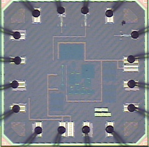 |
Name: HOURGLASS |
| Technology: TSMC 65-nm CMOS | |
| References: [1, 2] | |
| Description: mobility-based frequency reference |
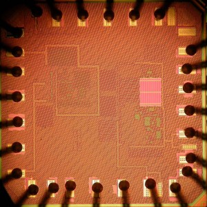 |
Name: SUNDIAL |
| Technology: TSMC 65-nm CMOS | |
| References: [3, 4, 5, 6] | |
| Description: bandgap-based temperature sensor and mobility-based frequency reference |
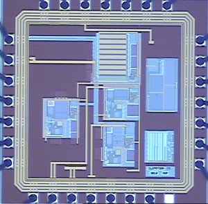 |
Name: CLEPSYDRA |
| Technology: SSMC 0.16-μum CMOS | |
| References: [7] | |
| Description: mobility-based frequency reference |
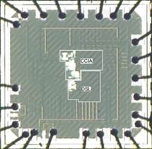 |
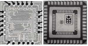
Name: BIOIA |
| Technology:TSMC 65-nm CMOS | |
| References: [8, 9, 10] | |
| Description: instrumentation amplifiers for biopotential applications |
 |
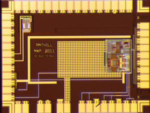
Name: LVINK |
| Technology: SSMC 0.16-μum CMOS | |
| References: [11] | |
| Description: capacitive MEMS microphone read-out |
 |
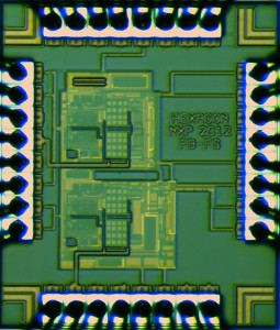
Name: ANTHILL |
| Technology: SSMC 0.16-μum CMOS | |
| References: [12] | |
| Description: ANalog-To-Digital Homogeneous Interface with Low area and Low latency (ANTHILL); 3-channel multiplexed ΣΔ ADC |
 |
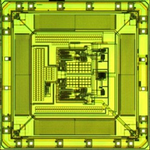
Name: HEXAGON |
| Technology: SSMC 0.16-μum CMOS | |
| References: [13] | |
| Description: 2-channel instrumentation amplifier with accurate gain matching |
 |
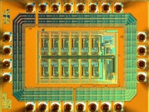
Name: |
| Technology: SSMC 0.16-μum CMOS | |
| References: [14] | |
| Description: wind sensor |
 |
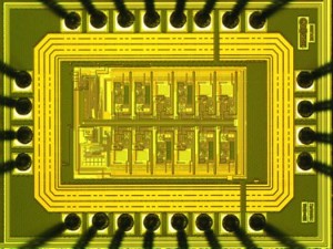
Name: MEERKAT |
| Technology: SSMC 0.16-μum CMOS | |
| References: [15] | |
| Description: thermal-diffusivity-based temperature sensor |
 |
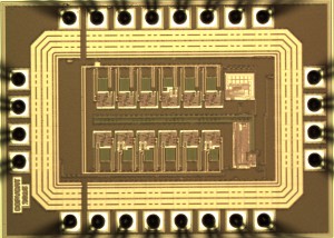
Name: HORSE |
| Technology: SSMC 0.16-μum CMOS | |
| References: [16] | |
| Description: thermal-diffusivity-based temperature sensor |
 |
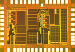
Name: |
| Technology: SSMC 0.16-μum CMOS | |
| References: [17] | |
| Description: mobility-based frequency reference |
 |
Name: QUIET |
| Technology: SSMC 0.16-μum CMOS | |
| References: [18, 19] | |
| Description: cryogenic low-noise amplifier |
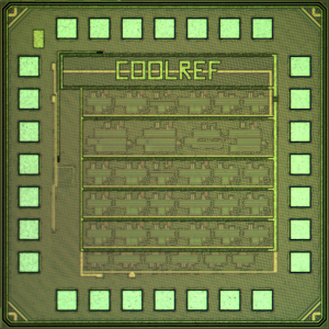 |
Name: COOLREF |
| Technology: TSMC 40-nm CMOS | |
| References: [20] | |
| Description: voltage references operating from 4 K up to 400 K |
References
[1] ![[doi]](http://www.fabiosebastiano.org/wp/wp-content/plugins/papercite/img/external.png) F. Sebastiano, L. J. Breems, K. A. A. Makinwa, S. Drago, D. M. W. Leenaerts, and B. Nauta, “A Low-Voltage Mobility-Based Frequency Reference for Crystal-Less ULP Radios,” in Proc. European Solid-State Circuits Conference, Edinburgh, UK, 2008, pp. 306-309.
F. Sebastiano, L. J. Breems, K. A. A. Makinwa, S. Drago, D. M. W. Leenaerts, and B. Nauta, “A Low-Voltage Mobility-Based Frequency Reference for Crystal-Less ULP Radios,” in Proc. European Solid-State Circuits Conference, Edinburgh, UK, 2008, pp. 306-309.
[Bibtex]
[Bibtex]
@inproceedings{mine:esscirc_2008_mobility,
title="A Low-Voltage Mobility-Based Frequency Reference for Crystal-Less {ULP} Radios",
author="Fabio Sebastiano and Lucien J. Breems and Kofi A.A. Makinwa and Salvatore Drago and Domine M.W. Leenaerts and Bram Nauta",
booktitle="Proc. {European Solid-State Circuits Conference}",
year="2008",
pages="306 - 309",
month=sep # {15--19},
address="Edinburgh, UK",
abstract={The design of a 100 kHz frequency reference based on the electron mobility in a MOS transistor is presented. The proposed low-voltage low-power circuit requires no off-chip components, making it suitable for Wireless Sensor Networks (WSN) applications. After one-point calibration the spread of its output frequency is less than 1.1% (3σ) over the temperature range from -22 °C to 85 °C. Fabricated in a baseline 65-nm CMOS technology, the frequency reference occupies 0.11 mm² and draws 34 µA from a 1.2-V supply at room temperature.},
keywords={CMOS integrated circuits;MOSFET circuits;electron mobility;integrated circuit design;low-power electronics;mobile radio;wireless sensor networks;MOS transistor;crystal less ULP radios;electron mobility;frequency 100 kHz;low voltage mobility based frequency reference;off-chip components;one point calibration;size 65 nm;temperature -22 degC to 85 degC;voltage 1.2 V;wireless sensor networks;CMOS technology;Calibration;Circuits;Energy consumption;Frequency;Oscillators;Silicon;Temperature distribution;Temperature sensors;Wireless sensor networks},
doi={10.1109/ESSCIRC.2008.4681853},
ISSN={1930-8833}
}
[2] ![[doi]](http://www.fabiosebastiano.org/wp/wp-content/plugins/papercite/img/external.png) F. Sebastiano, L. J. Breems, K. A. A. Makinwa, S. Drago, D. M. W. Leenaerts, and B. Nauta, “A Low-Voltage Mobility-Based Frequency Reference for Crystal-Less ULP Radios,” IEEE J. Solid-State Circuits, vol. 44, iss. 7, pp. 2002-2009, 2009.
F. Sebastiano, L. J. Breems, K. A. A. Makinwa, S. Drago, D. M. W. Leenaerts, and B. Nauta, “A Low-Voltage Mobility-Based Frequency Reference for Crystal-Less ULP Radios,” IEEE J. Solid-State Circuits, vol. 44, iss. 7, pp. 2002-2009, 2009.
[Bibtex]
[Bibtex]
@article{mine:jssc_2009_mobility,
title="A Low-Voltage Mobility-Based Frequency Reference for Crystal-Less {ULP} Radios",
author="Fabio Sebastiano and Lucien J. Breems and Kofi A.A. Makinwa and Salvatore Drago and Domine M.W. Leenaerts and Bram Nauta",
journal=IEEE_J_JSSC,
year={2009},
month=jul,
volume={44},
number={7},
pages={2002 -2009},
abstract={The design of a 100 kHz frequency reference based on the electron mobility in a MOS transistor is presented. The proposed low-voltage low-power circuit requires no off-chip components, making it suitable for application in wireless sensor networks (WSN). After a single-point calibration, the spread of its output frequency is less than 1.1% (3σ) over the temperature range from -22 °C to 85 °C . Fabricated in a baseline 65 nm CMOS technology, the frequency reference circuit occupies 0.11 mm² and draws 34 µA from a 1.2 V supply at room temperature.},
keywords={CMOS integrated circuits;MOSFET;wireless sensor networks;CMOS technology;MOS transistor;crystal-less ULP radios;current 34 muA;electron mobility;frequency 100 kHz;low-voltage low-power circuit;low-voltage mobility-based frequency reference;size 65 nm;temperature -22 degC to 85 degC;temperature 293 K to 298 K;voltage 1.2 V;wireless sensor networks;CMOS technology;Circuits;Electron mobility;Energy consumption;Frequency synchronization;MOSFETs;Oscillators;Silicon;Temperature sensors;Wireless sensor networks;CMOS analog integrated circuits;Charge carrier mobility;crystal-less clock;low voltage;relaxation oscillators;ultra-low power;wireless sensor networks},
doi={10.1109/JSSC.2009.2020247},
ISSN={0018-9200},
}
[3] ![[doi]](http://www.fabiosebastiano.org/wp/wp-content/plugins/papercite/img/external.png) F. Sebastiano, L. J. Breems, K. Makinwa, S. Drago, D. M. W. Leenaerts, and B. Nauta, “A 1.2V 10µW NPN-based temperature sensor in 65nm CMOS with an inaccuracy of ±0.2°C (3σ) from -70°C to 125°C,” in International Solid-state Circuits Conference Digest of Technical Papers, San Francisco, CA, 2010, pp. 312-313.
F. Sebastiano, L. J. Breems, K. Makinwa, S. Drago, D. M. W. Leenaerts, and B. Nauta, “A 1.2V 10µW NPN-based temperature sensor in 65nm CMOS with an inaccuracy of ±0.2°C (3σ) from -70°C to 125°C,” in International Solid-state Circuits Conference Digest of Technical Papers, San Francisco, CA, 2010, pp. 312-313.
[Bibtex]
[Bibtex]
@inproceedings{mine:isscc_2010_temp_sens,
author = "Fabio Sebastiano and Lucien J. Breems and Kofi Makinwa and Salvatore Drago and Domine M. W. Leenaerts and Bram Nauta",
month = feb # {7--11},
year = "2010",
title = "A {1.2V} {10µW} {NPN}-based temperature sensor in 65nm {CMOS} with an inaccuracy of ±0.2°{C} (3σ) from -70°{C} to 125°{C}",
booktitle={International Solid-state Circuits Conference Digest of Technical Papers},
pages="312 - 313",
address="San Francisco, CA",
abstract={A temperature sensor utilizing NPN transistors has been realized in a 65 nm CMOS process. It achieves a batch-calibrated inaccuracy of ±0.5°C (3σ) and a trimmed inaccuracy of ±0.2°C (3σ) from -70°C to 125°C The sensor draws 8.3 µA from a 1.2 V supply and occupies an area of 0.1 mm².},
keywords={CMOS integrated circuits;signal processing equipment;temperature sensors;CMOS technology;batch calibrated inaccuracy;current 8.3 �A;power 10 �W;size 65 nm;temperature -70 C to 125 C;temperature sensor;voltage 1.2 V;CMOS technology;Pipelines;Robustness;Sampling methods;Switches;Tail;Temperature sensors;Testing;Timing;Voltage},
doi={10.1109/ISSCC.2010.5433895},
ISSN={0193-6530}
}[4] ![[doi]](http://www.fabiosebastiano.org/wp/wp-content/plugins/papercite/img/external.png) F. Sebastiano, L. J. Breems, K. Makinwa, S. Drago, D. M. W. Leenaerts, and B. Nauta, “A 65-nm CMOS temperature-compensated mobility-based frequency reference for Wireless Sensor Networks,” in Proc. European Solid-State Circuits Conference, Sevilla, Spain, 2010, pp. 102-105.
F. Sebastiano, L. J. Breems, K. Makinwa, S. Drago, D. M. W. Leenaerts, and B. Nauta, “A 65-nm CMOS temperature-compensated mobility-based frequency reference for Wireless Sensor Networks,” in Proc. European Solid-State Circuits Conference, Sevilla, Spain, 2010, pp. 102-105.
[Bibtex]
[Bibtex]
@INPROCEEDINGS{mine:esscirc_2010_mobility_comp,
author = "Fabio Sebastiano and Lucien J. Breems and Kofi Makinwa and Salvatore Drago and Domine M. W. Leenaerts and Bram Nauta",
booktitle="Proc. {European Solid-State Circuits Conference}",
title="A 65-nm {CMOS} temperature-compensated mobility-based frequency reference for Wireless Sensor Networks",
year={2010},
month=sep # {14--16},
pages={102 - 105},
address="Sevilla, Spain",
abstract={For the first time, a temperature-compensated CMOS frequency reference based on the electron mobility in a MOS transistor is presented. Over the temperature range from -55 °C to 125 °C, its frequency spread is less than ±0.5% after a two-point trim and less than ±2.7% after a one-point trim. These results make it suitable for use in Wireless Sensor Network nodes. Fabricated in a baseline 65-nm CMOS process, the 150 kHz frequency reference occupies 0.2 mm² and draws 42.6 µA from a 1.2-V supply at room temperature.},
keywords={CMOS integrated circuits;MOSFET;electron mobility;wireless sensor networks;CMOS temperature-compensated mobility;MOS transistor;current 42.6 muA;electron mobility;frequency 150 kHz;frequency reference;size 65 nm;temperature -55 C to 125 C;voltage 1.2 V;wireless sensor network;Accuracy;CMOS integrated circuits;Calibration;Oscillators;Temperature measurement;Temperature sensors;Wireless sensor networks},
doi={10.1109/ESSCIRC.2010.5619792},
ISSN={1930-8833}
}
[5] ![[doi]](http://www.fabiosebastiano.org/wp/wp-content/plugins/papercite/img/external.png) F. Sebastiano, L. J. Breems, K. Makinwa, S. Drago, D. M. W. Leenaerts, and B. Nauta, “A 1.2-V 10-µW NPN-Based Temperature Sensor in 65-nm CMOS With an Inaccuracy of 0.2 °C (3σ) From -70 °C to 125 °C,” IEEE J. Solid-State Circuits, vol. 45, iss. 12, pp. 2591-2601, 2010.
F. Sebastiano, L. J. Breems, K. Makinwa, S. Drago, D. M. W. Leenaerts, and B. Nauta, “A 1.2-V 10-µW NPN-Based Temperature Sensor in 65-nm CMOS With an Inaccuracy of 0.2 °C (3σ) From -70 °C to 125 °C,” IEEE J. Solid-State Circuits, vol. 45, iss. 12, pp. 2591-2601, 2010.
[Bibtex]
[Bibtex]
@ARTICLE{mine:jssc_2010_temp_sens,
author = "Fabio Sebastiano and Lucien J. Breems and Kofi Makinwa and Salvatore Drago and Domine M. W. Leenaerts and Bram Nauta",
journal=IEEE_J_JSSC,
title="A 1.2-{V} 10-µ{W} {NPN}-Based Temperature Sensor in 65-nm {CMOS} With an Inaccuracy of 0.2 °{C} (3σ) From -70 °{C} to 125 °{C}",
year={2010},
month=dec,
volume={45},
number={12},
pages={2591 - 2601},
abstract={An NPN-based temperature sensor with digital output has been realized in a 65-nm CMOS process. It achieves a batch-calibrated inaccuracy of (3σ) and a trimmed inaccuracy of (3σ) over the temperature range from -70 °C to 125 °C. This performance is obtained by the use of NPN transistors as sensing elements, the use of dynamic techniques, i.e., correlated double sampling and dynamic element matching, and a single room-temperature trim. The sensor draws 8.3 µA from a 1.2-V supply and occupies an area of 0.1 mm².},
keywords={CMOS integrated circuits;correlation methods;signal sampling;temperature sensors;CMOS;correlated double sampling;dynamic element matching;npn transistor;power 10 muW;size 65 nm;temperature -70 C to 125 C;temperature sensor;voltage 1.2 V;CMOS analog integrated circuits;CMOS process;Intelligent sensors;Sigma delta modulation;Temperature sensors;CMOS analog integrated circuits;sigma-delta modulation;smart sensors;temperature sensors},
doi={10.1109/JSSC.2010.2076610},
ISSN={0018-9200}
}
[6] ![[doi]](http://www.fabiosebastiano.org/wp/wp-content/plugins/papercite/img/external.png) F. Sebastiano, L. J. Breems, K. Makinwa, S. Drago, D. M. W. Leenaerts, and B. Nauta, “A 65-nm CMOS temperature-compensated mobility-based frequency reference for Wireless Sensor Networks,” IEEE J. Solid-State Circuits, vol. 46, iss. 7, pp. 1544-1552, 2011.
F. Sebastiano, L. J. Breems, K. Makinwa, S. Drago, D. M. W. Leenaerts, and B. Nauta, “A 65-nm CMOS temperature-compensated mobility-based frequency reference for Wireless Sensor Networks,” IEEE J. Solid-State Circuits, vol. 46, iss. 7, pp. 1544-1552, 2011.
[Bibtex]
[Bibtex]
@ARTICLE{mine:jssc_2011_mobility_comp,
author = "Fabio Sebastiano and Lucien J. Breems and Kofi Makinwa and Salvatore Drago and Domine M. W. Leenaerts and Bram Nauta",
journal=IEEE_J_JSSC,
title="A 65-nm {CMOS} temperature-compensated mobility-based frequency reference for Wireless Sensor Networks",
year={2011},
month=jul,
volume={46},
number={7},
pages={1544 - 1552},
abstract={A temperature-compensated CMOS frequency reference based on the electron mobility in a MOS transistor is presented. Over the temperature range from -55 °C to 125 °C, the frequency spread of the complete reference is less than ±0.5% after a two-point trim and less than ±2.7% after a one-point trim. These results make it suitable for use in Wireless Sensor Network nodes. Fabricated in a baseline 65-nm CMOS process, the 150 kHz frequency reference occupies 0.2 mm² and draws 42.6 µA from a 1.2-V supply at room temperature.},
keywords={CMOS integrated circuits;compensation;electron mobility;wireless sensor networks;MOS transistor;current 42.6 muA;electron mobility;mobility-based frequency reference;size 65 nm;temperature -55 degC to 125 degC;temperature-compensated CMOS frequency reference;two-point trim;voltage 1.2 V;wireless sensor networks;Accuracy;Frequency conversion;Oscillators;Temperature;Temperature measurement;Temperature sensors;Wireless sensor networks;CMOS integrated circuits;Charge carrier mobility;MOSFET;crystal-less clock;frequency reference;low voltage;sigma-delta modulation;smart sensors;temperature compensation;temperature sensors;ultra-low power;wireless sensor networks},
doi={10.1109/JSSC.2011.2143630},
ISSN={0018-9200}
}
[7] ![[doi]](http://www.fabiosebastiano.org/wp/wp-content/plugins/papercite/img/external.png) F. Sebastiano, L. J. Breems, K. Makinwa, S. Drago, D. M. W. Leenaerts, and B. Nauta, “Effects of Packaging and Process Spread on a Mobility-Based Frequency Reference in 0.16-µm CMOS,” in Proc. European Solid-State Circuits Conference, Helsinki, Finland, 2011, pp. 511-514.
F. Sebastiano, L. J. Breems, K. Makinwa, S. Drago, D. M. W. Leenaerts, and B. Nauta, “Effects of Packaging and Process Spread on a Mobility-Based Frequency Reference in 0.16-µm CMOS,” in Proc. European Solid-State Circuits Conference, Helsinki, Finland, 2011, pp. 511-514.
[Bibtex]
[Bibtex]
@INPROCEEDINGS{mine:esscirc_2011_mobility_cmos14,
author = "Fabio Sebastiano and Lucien J. Breems and Kofi Makinwa and Salvatore Drago and Domine M. W. Leenaerts and Bram Nauta",
booktitle="Proc. {European Solid-State Circuits Conference}",
title="Effects of Packaging and Process Spread on a Mobility-Based Frequency Reference in 0.16-µm {CMOS}",
year={2011},
month=sep # {12-16},
address="Helsinki, Finland",
pages={511 - 514},
abstract={In this paper, we explore the robustness of frequency references based on the electron mobility in a MOS transistor by implementing them with both thin-oxide and thick-oxide MOS transistors in a 0.16-µm CMOS process, and by testing samples packaged in both ceramic and plastic packages. The proposed low-voltage low-power circuit requires no off-chip components, making it suitable for applications requiring fully integrated solutions, such as Wireless Sensor Networks. Over the temperature range from -55 °C to 125 °C, its frequency spread is less than ±1% (3σ) after a one-point trim. Fabricated in a baseline 0.16-µm CMOS process, the 50 kHz frequency reference occupies 0.06 mm² and, at room temperature, its consumption with a 1.2-V supply is less than 17 µW.},
keywords={CMOS integrated circuits;MOSFET;ceramic packaging;electron mobility;low-power electronics;plastic packaging;reference circuits;wireless sensor networks;CMOS process;ceramic packages;electron mobility;frequency 50 kHz;low-voltage low-power circuit;mobility-based frequency reference;off-chip components;packaging;plastic packages;process spread;size 0.16 mum;temperature -55 degC to 125 degC;temperature 293 K to 298 K;thick-oxide MOS transistors;thin-oxide MOS transistors;voltage 1.2 V;wireless sensor networks;Accuracy;Ceramics;Oscillators;Plastics;Temperature distribution;Temperature measurement;Transistors},
doi={10.1109/ESSCIRC.2011.6044934},
ISSN={1930-8833}
}
[8] ![[doi]](http://www.fabiosebastiano.org/wp/wp-content/plugins/papercite/img/external.png) Q. Fan, F. Sebastiano, J. H. Huijsing, and K. A. A. Makinwa, “A 1.8µW 1-µV-offset capacitively-coupled chopper instrumentation amplifier in 65nm CMOS,” in Proc. European Solid-State Circuits Conference, Sevilla, Spain, 2010, pp. 170-173.
Q. Fan, F. Sebastiano, J. H. Huijsing, and K. A. A. Makinwa, “A 1.8µW 1-µV-offset capacitively-coupled chopper instrumentation amplifier in 65nm CMOS,” in Proc. European Solid-State Circuits Conference, Sevilla, Spain, 2010, pp. 170-173.
[Bibtex]
[Bibtex]
@INPROCEEDINGS{mine:esscirc_2010_qinwen,
author="Qinwen Fan and Fabio Sebastiano and Johan H. Huijsing and Kofi A.A. Makinwa",
booktitle="Proc. {European Solid-State Circuits Conference}",
title="A 1.8µ{W} 1-µV-offset capacitively-coupled chopper instrumentation amplifier in 65nm {CMOS}",
year={2010},
month=sep # {14--16},
address="Sevilla, Spain",
pages={170 - 173},
abstract={This paper describes a precision capacitively-coupled chopper instrumentation amplifier (CCIA). It achieves 1µV offset, 134dB CMRR, 120dB PSRR, 0.16% gain accuracy and a noise efficiency factor (NEF) of 3.1, which is more than 3x better than state-of-the-art. It has a rail-to-rail DC common-mode (CM) input range. Furthermore, a positive feedback loop (PFL) is used to boost the input impedance, and a ripple reduction loop (RRL) is used to reduce the ripple associated with chopping. The CCIA occupies only 0.1mm² in a 65nm CMOS technology. It can operate from a 1V supply, from which it draws only 1.8µA.},
keywords={CMOS integrated circuits;instrumentation amplifiers;CMOS;input impedance;noise efficiency factor;positive feedback loop;precision capacitively-coupled chopper instrumentation amplifier;rail-to-rail DC common-mode input range;ripple reduction loop;size 65 nm;Accuracy;Choppers;Impedance;Instruments;Noise;Resistors;Topology},
doi={10.1109/ESSCIRC.2010.5619902},
ISSN={1930-8833}
}
[9] ![[doi]](http://www.fabiosebastiano.org/wp/wp-content/plugins/papercite/img/external.png) Q. Fan, F. Sebastiano, J. H. Huijsing, and K. A. A. Makinwa, “A 2.1 µW Area-Efficient Capacitively-Coupled Chopper Instrumentation Amplifier for ECG Applications in 65 nm CMOS,” in Proc. Asian Solid-State Circuits Conference, Beijing, China, 2010, pp. 1-4.
Q. Fan, F. Sebastiano, J. H. Huijsing, and K. A. A. Makinwa, “A 2.1 µW Area-Efficient Capacitively-Coupled Chopper Instrumentation Amplifier for ECG Applications in 65 nm CMOS,” in Proc. Asian Solid-State Circuits Conference, Beijing, China, 2010, pp. 1-4.
[Bibtex]
[Bibtex]
@INPROCEEDINGS{mine:asscc_2010_qinwen,
author="Qinwen Fan and Fabio Sebastiano and Johan H. Huijsing and Kofi A.A. Makinwa",
booktitle="Proc. {Asian Solid-State Circuits Conference}",
title="A 2.1 µ{W} Area-Efficient Capacitively-Coupled Chopper Instrumentation Amplifier for ECG Applications in 65 nm {CMOS}",
year={2010},
month=nov # {8--10},
address="Beijing, China",
pages={1 - 4},
abstract={This paper describes a capacitively-coupled chopper instrumentation amplifier for use in electrocardiography (ECG). The amplifier's gain is accurately defined by a capacitive feedback network, while a DC servo loop rejects the DC offset generated by the electrode-tissue interface. The high-pass corner frequency established by the servo loop is realized by an area-efficient switched-capacitor integrator. Additional feedback loops are employed to boost the amplifier's input-impedance to 80 MΩ and to suppress the chopper ripple. Implemented in a 65 nm CMOS technology, the amplifier draws 2.1 µA from a 1 V supply and occupies 0.2 mm².},
keywords={CMOS integrated circuits;amplifiers;biomedical electrodes;choppers (circuits);electrocardiography;CMOS technology;DC servo loop;ECG application;area efficient chopper instrumentation amplifier;capacitive feedback network;capacitively coupled chopper instrumentation amplifier;electrocardiography;electrode-tissue interface;power 2.1 muW;switched capacitor integrator;Choppers;DSL;Earth Observing System;Electrocardiography;Impedance;Instruments;Noise},
doi={10.1109/ASSCC.2010.5716624}
}
[10] ![[doi]](http://www.fabiosebastiano.org/wp/wp-content/plugins/papercite/img/external.png) Q. Fan, F. Sebastiano, J. H. Huijsing, and K. A. A. Makinwa, “A 1.8 µW 60 nV/√Hz Capacitively-Coupled Chopper Instrumentation Amplifier in 65 nm CMOS for Wireless Sensor Nodes,” IEEE J. Solid-State Circuits, vol. 46, iss. 7, pp. 1534-1543, 2011.
Q. Fan, F. Sebastiano, J. H. Huijsing, and K. A. A. Makinwa, “A 1.8 µW 60 nV/√Hz Capacitively-Coupled Chopper Instrumentation Amplifier in 65 nm CMOS for Wireless Sensor Nodes,” IEEE J. Solid-State Circuits, vol. 46, iss. 7, pp. 1534-1543, 2011.
[Bibtex]
[Bibtex]
@ARTICLE{mine:jssc_2011_qinwen,
author="Qinwen Fan and Fabio Sebastiano and Johan H. Huijsing and Kofi A.A. Makinwa",
journal=IEEE_J_JSSC,
title="A 1.8 µ{W} 60 nV/√{Hz} Capacitively-Coupled Chopper Instrumentation Amplifier in 65 nm {CMOS} for Wireless Sensor Nodes",
year={2011},
month=jul,
volume={46},
number={7},
pages={1534 - 1543},
abstract={This paper presents a low-power precision instrumentation amplifier intended for use in wireless sensor nodes. It employs a capacitively-coupled chopper topology to achieve a rail-to-rail input common-mode range as well as high power efficiency. A positive feedback loop is employed to boost its input impedance, while a ripple reduction loop suppresses the chopping ripple. To facilitate bio-potential sensing, an optional DC servo loop may be employed to suppress electrode offset. The IA achieves 1 µV offset, 0.16% gain inaccuracy, 134 dB CMRR, 120 dB PSRR and a noise efficiency factor of 3.3. The instrumentation amplifier was implemented in a 65 nm CMOS technology. It occupies only 0.1 mm² chip area (0.2 mm² with the DC servo loop) and consumes 1.8 µA current (2.1 µA with the DC servo loop) from a 1 V supply.},
keywords={CMOS integrated circuits;choppers (circuits);instrumentation amplifiers;wireless sensor networks;CMOS technology;CMRR;DC servo loop;PSRR;biopotential sensing;capacitively-coupled chopper instrumentation amplifier;chopping ripple;current 1.8 muA;electrode offset suppression;low-power precision instrumentation amplifier;noise efficiency factor;positive feedback loop;power 1.8 muW;rail-to-rail input common-mode range;ripple reduction loop;size 65 nm;voltage 1 V;wireless sensor nodes;Capacitors;Choppers;Impedance;Noise;Sensors;Topology;Wireless sensor networks;Bio-signal sensing;chopping;high power efficiency;low offset;low power;precision amplifier;wireless sensor nodes},
doi={10.1109/JSSC.2011.2143610},
ISSN={0018-9200}
}
[11] ![[doi]](http://www.fabiosebastiano.org/wp/wp-content/plugins/papercite/img/external.png) S. Ersoy, R. H. M. van Veldhoven, F. Sebastiano, and K. Reimann, “A 0.25mm² AC-Biased MEMS Microphone Interface with 58dBA SNR,” in International Solid-state Circuits Conference Digest of Technical Papers, San Francisco, CA, 2013, pp. 382-383.
S. Ersoy, R. H. M. van Veldhoven, F. Sebastiano, and K. Reimann, “A 0.25mm² AC-Biased MEMS Microphone Interface with 58dBA SNR,” in International Solid-state Circuits Conference Digest of Technical Papers, San Francisco, CA, 2013, pp. 382-383.
[Bibtex]
[Bibtex]
@inproceedings{mine:isscc_2013_selcuk,
author = "Sel\c{c}uk Ersoy and Robert H.M. van Veldhoven and Fabio Sebastiano and Klaus Reimann",
month = feb # {17--21},
year = "2013",
title="A 0.25mm² {AC}-Biased {MEMS} Microphone Interface with {58dBA SNR}",
booktitle={International Solid-state Circuits Conference Digest of Technical Papers},
pages="382-383",
address="San Francisco, CA",
abstract={Capacitive MEMS microphone roadmaps are mainly driven by increasing SNR and reducing size/cost. This requires smaller microphones, ASICs with lower noise and smaller area, and cheaper packaging. Because of fundamental limitations, traditional DC-biased microphones will have difficulty following these trends. This paper proposes an AC-biasing scheme, which leads to a significant reduction in ASIC size and module packaging cost.},
keywords={AC machines;DC machines;capacitance;electronics packaging;micromechanical devices;microphones;AC-biased MEMS microphone interface;AC-biasing scheme;ASIC size reduction;DC-biased microphone;SNR;capacitive MEMS microphone roadmap;module packaging cost;noise},
doi={10.1109/ISSCC.2013.6487779},
ISSN={0193-6530}
}
[12] ![[doi]](http://www.fabiosebastiano.org/wp/wp-content/plugins/papercite/img/external.png) F. Sebastiano and R. H. M. van Veldhoven, “A 0.1-mm² 3-Channel Area-Optimized ΣΔ ADC in 0.16-µm CMOS with 20-kHz BW and 86-dB DR,” in Proc. European Solid-State Circuits Conference, Bucharest, Romania, 2013, pp. 375-378.
F. Sebastiano and R. H. M. van Veldhoven, “A 0.1-mm² 3-Channel Area-Optimized ΣΔ ADC in 0.16-µm CMOS with 20-kHz BW and 86-dB DR,” in Proc. European Solid-State Circuits Conference, Bucharest, Romania, 2013, pp. 375-378.
[Bibtex]
[Bibtex]
@INPROCEEDINGS{mine:esscirc_2013_sigmadelta,
author = "Fabio Sebastiano and Robert H.M. van Veldhoven",
booktitle="Proc. {European Solid-State Circuits Conference}",
title="A 0.1-mm² 3-Channel Area-Optimized ΣΔ {ADC} in 0.16-µm {CMOS} with {20-kHz} {BW} and {86-dB DR}",
year={2013},
month=sep # {16--20},
address="Bucharest, Romania",
pages={375 - 378},
abstract={Front-ends for automotive sensors must digitize multiple channels with high resolution while minimizing their silicon area to save costs. Both channel latency and inter-channel gain mismatch must be minimized to be able to serve multiple sensor applications, ranging from ABS to power steering, with the same front-end. The proposed S? ADC simultaneously digitizes 3 channels, each with a DR of 86 dB over a 20-kHz BW using a 75-MHz clock. Channel latency is <40 ns and inter-channel gain mismatch is <0.2%. The ADC occupies only 0.1 mm² in a 0.16-µm CMOS process. The small area is enabled by channel multiplexing, allowing component sharing among the channels, and by the large oversampling ratio (OSR), allowing for smaller capacitors.},
keywords={CMOS integrated circuits;analogue-digital conversion;automotive electronics;delta-sigma modulation;3-channel area-optimized S? ADC;CMOS;automotive sensors;capacitors;channel latency;channel multiplexing;frequency 20 kHz;frequency 75 MHz;front-ends;inter-channel gain mismatch;oversampling ratio;size 0.16 mum;Capacitors;Crosstalk;Gain;Modulation;Multiplexing;Noise;Sensors},
doi={10.1109/ESSCIRC.2013.6649151},
ISSN={1930-8833}
}
[13] ![[doi]](http://www.fabiosebastiano.org/wp/wp-content/plugins/papercite/img/external.png) F. Sebastiano, F. Butti, R. H. M. van Veldhoven, and P. Bruschi, "A 0.07mm² 2-Channel Instrumentation Amplifier with 0.1% Gain Matching in 0.16µm CMOS," in International Solid-state Circuits Conference Digest of Technical Papers, San Francisco, CA, 2014, pp. 294-295.
F. Sebastiano, F. Butti, R. H. M. van Veldhoven, and P. Bruschi, "A 0.07mm² 2-Channel Instrumentation Amplifier with 0.1% Gain Matching in 0.16µm CMOS," in International Solid-state Circuits Conference Digest of Technical Papers, San Francisco, CA, 2014, pp. 294-295.
[Bibtex]
[Bibtex]
@inproceedings{mine:isscc_2014_amplifier,
author = "Fabio Sebastiano and Federico Butti and Robert H.M. van Veldhoven and Paolo Bruschi",
month = feb # {9--13},
year = "2014",
title="A 0.07mm² 2-Channel Instrumentation Amplifier with 0.1% Gain Matching in 0.16µm {CMOS}",
booktitle={International Solid-state Circuits Conference Digest of Technical Papers},
pages={294 - 295},
abstract={Extremely small-area sensor front-ends are required for cost-constrained automotive applications. Instrumentation amplifiers (IA) for such front-ends must process multi-channel sensor outputs and provide gain matching over the channels for proper sensor operation. Angular sensors are a typical example, in which the sine and cosine outputs of a resistive magnetic sensor must be processed with adequate gain matching to avoid unacceptable angular errors. This paper presents a 2-channel instrumentation amplifier in 0.16µm CMOS with 0.1% gain matching and occupying 0.035mm2 per channel. This represents a 13.3x area improvement with respect to state-of-the-art designs with similar gain accuracy [1]-[4], while maintaining low noise (18.7nV/√Hz), low offset (17µV) and high power efficiency (NEF=12.9). The accurate gain matching in a limited area is enabled by the adoption of a dynamic element matching (DEM) scheme and by the use of a high chopping frequency.},
keywords={CMOS integrated circuits;instrumentation amplifiers;2-channel instrumentation amplifier;CMOS;DEM scheme;IA;angular sensors;cosine outputs;cost-constrained automotive applications;dynamic element matching scheme;gain matching;high chopping frequency;multichannel sensor outputs;resistive magnetic sensor;sensor front-ends;sensor operation;size 0.16 mum;voltage 17 muV;Accuracy;CMOS integrated circuits;Gain measurement;Instruments;Noise measurement;Solid state circuits;Switches},
address="San Francisco, CA",
doi={10.1109/ISSCC.2014.6757440},
ISSN={0193-6530},
}
[14] ![[doi]](http://www.fabiosebastiano.org/wp/wp-content/plugins/papercite/img/external.png) W. Brevet, F. Sebastiano, and K. A. A. Makinwa, "A 25mW Smart CMOS Wind Sensor with Corner Heaters," in 41st Annual Conference of IEEE Industrial Electronics Society, Yokohama, Japan, 2015, pp. 1194-1199.
W. Brevet, F. Sebastiano, and K. A. A. Makinwa, "A 25mW Smart CMOS Wind Sensor with Corner Heaters," in 41st Annual Conference of IEEE Industrial Electronics Society, Yokohama, Japan, 2015, pp. 1194-1199.
[Bibtex]
[Bibtex]
@INPROCEEDINGS{mine:iecon_2015_wind_sensor,
author={Wouter Brevet and Fabio Sebastiano and Kofi A.A. Makinwa},
booktitle={41st Annual Conference of IEEE Industrial Electronics Society},
address="Yokohama, Japan",
title="A 25m{W} Smart {CMOS} Wind Sensor with Corner Heaters",
pages={001194-001199},
abstract={A smart CMOS thermal wind sensor has been optimized for commercial use. Optimizing the sensor chip's thermal design resulted in better area efficiency and improved thermal dynamics with respect to prior work. The latter simplifies the off-chip decimation of the sensor's bitstream outputs. Moreover, by realizing more logic on-chip, the number of bond wires has been reduced by 33%, to 8, thus reducing manufacturing costs. Fabricated in a standard 0.7�m CMOS process, the sensor chip occupies 4�4mm2 and consumes 25mW of heating power, while achieving an inaccuracy of �6% (speed) and �2� (direction), for wind speeds between 4 and 25m/s.},
keywords={CMOS integrated circuits;heating;intelligent sensors;wind power;wires (electric);corner heater;logic on-chip;power 25 mW;sensor bitstream output off-chip decimation;sensor chip thermal design;size 0.7 mum;smart CMOS thermal wind sensor;standard CMOS process;Clocks;Frequency modulation;Heating;Thermal sensors;Wind speed;Electrothermal filter (ETF);Smart wind sensor;Thermal sensors;thermal sigma-delta modulatiom},
doi={10.1109/IECON.2015.7392262},
month={Nov},
year="2015"
}[15] ![[doi]](http://www.fabiosebastiano.org/wp/wp-content/plugins/papercite/img/external.png) U. Sonmez, R. Quan, F. Sebastiano, and K. A. A. Makinwa, "A 0.008-mm² area-optimized thermal-diffusivity-based temperature sensor in 160-nm CMOS for SoC thermal monitoring," in Proc. European Solid-State Circuits Conference, Venice, Italy, 2014, pp. 395-398.
U. Sonmez, R. Quan, F. Sebastiano, and K. A. A. Makinwa, "A 0.008-mm² area-optimized thermal-diffusivity-based temperature sensor in 160-nm CMOS for SoC thermal monitoring," in Proc. European Solid-State Circuits Conference, Venice, Italy, 2014, pp. 395-398.
[Bibtex]
[Bibtex]
@INPROCEEDINGS{mine:esscirc_2014_TD_sensor,
author = "Ugur Sonmez and Rui Quan and Fabio Sebastiano and Kofi. A. A. Makinwa",
booktitle="Proc. {European Solid-State Circuits Conference}",
title={A 0.008-mm² area-optimized thermal-diffusivity-based temperature sensor in 160-nm {CMOS} for {SoC} thermal monitoring},
year={2014},
month=sep # {22--26},
address="Venice, Italy",
pages={395-398},
abstract={An array of temperature sensors based on the temperature-dependent thermal diffusivity of bulk silicon has been realized in a standard 160-nm CMOS process. The sensors achieve an inaccuracy of ±2.4 °C (3σ) from -40 to 125 °C with no trimming and ±0.65 °C (3σ) with a one temperature trim. Each sensor occupies 0.008 mm², and achieves a resolution of 0.21 °C (rms) at 1 kSa/s. This combination of accuracy, speed, and small size makes such sensors well suited for thermal monitoring in microprocessors and other systems-on-chip.},
keywords={CMOS integrated circuits;system-on-chip;temperature measurement;temperature sensors;thermal diffusivity;SoC thermal monitoring;area-optimized thermal-diffusivity-based temperature sensor;bulk silicon;microprocessors;size 160 nm;standard CMOS process;systems-on-chip;temperature-dependent thermal diffusivity;thermal monitoring;Accuracy;Heating;System-on-chip;Temperature measurement;Temperature sensors},
doi={10.1109/ESSCIRC.2014.6942105},
ISSN={1930-8833}
}
[16] ![[doi]](http://www.fabiosebastiano.org/wp/wp-content/plugins/papercite/img/external.png) R. Quan, U. Sonmez, and K. M. A. A. Fabio Sebastiano and, "A 4600µm² 1.5°C (3σ) 0.9kS/s thermal-diffusivity temperature sensor with VCO-based readout," in International Solid-state Circuits Conference Digest of Technical Papers, San Francisco, CA, 2015, pp. 488-489.
R. Quan, U. Sonmez, and K. M. A. A. Fabio Sebastiano and, "A 4600µm² 1.5°C (3σ) 0.9kS/s thermal-diffusivity temperature sensor with VCO-based readout," in International Solid-state Circuits Conference Digest of Technical Papers, San Francisco, CA, 2015, pp. 488-489.
[Bibtex]
[Bibtex]
@INPROCEEDINGS{mine:isscc_2015_TD_sensor,
author={Rui Quan and Ugur Sonmez and Fabio Sebastiano and, Kofi A.A. Makinwa},
booktitle={International Solid-state Circuits Conference Digest of Technical Papers},
address="San Francisco, CA",
title={A 4600µm² 1.5°C (3σ) 0.9{kS/s} thermal-diffusivity temperature sensor with VCO-based readout},
year={2015},
month={Feb},
pages={488 - 489},
abstract={This paper presents a highly digital thermal-diffusivity temperature sensor in 0.16µm CMOS for SoC thermal monitoring. The sensor occupies only 4600µm², which is the smallest for designs above 32nm and is one of the smallest ever reported. It also achieves ±1.5°C (3σ, single trim) inaccuracy and 0.6$^circ$C resolution at a 0.9kS/s sampling rate. This small area implementation is mainly enabled by the adoption of a VCO-based phase-domain ADC whose area is 70% digital.},
keywords={Accuracy;CMOS integrated circuits;Modulation;Radiation detectors;Temperature sensors},
doi={10.1109/ISSCC.2015.7063139},}
[17] ![[doi]](http://www.fabiosebastiano.org/wp/wp-content/plugins/papercite/img/external.png) J. Angevare, L. Pedalà, U. Sonmez, F. Sebastiano, and K. A. A. Makinwa, "A 2800-µm² Thermal-Diffusivity Temperature Sensor with VCO-Based Readout in 160-nm CMOS," in Asian Solid-state Circuits Conference Digest of Technical Papers, Xiamen, China, 2015, pp. 1-4.
J. Angevare, L. Pedalà, U. Sonmez, F. Sebastiano, and K. A. A. Makinwa, "A 2800-µm² Thermal-Diffusivity Temperature Sensor with VCO-Based Readout in 160-nm CMOS," in Asian Solid-state Circuits Conference Digest of Technical Papers, Xiamen, China, 2015, pp. 1-4.
[Bibtex]
[Bibtex]
@INPROCEEDINGS{mine:asscc_2015_TD_sensor,
author={Jan Angevare and Lorenzo Pedalà and Ugur Sonmez and Fabio Sebastiano and Kofi A.A. Makinwa},
booktitle={Asian Solid-state Circuits Conference Digest of Technical Papers},
address="Xiamen, China",
title="A 2800-µm² Thermal-Diffusivity Temperature Sensor with {VCO}-Based Readout in 160-nm {CMOS}",
year={2015},
pages={1-4},
abstract={A highly digital temperature sensor based on the temperature-dependent thermal diffusivity of bulk silicon has been realized in a standard 160-nm CMOS process. The sensor achieves an inaccuracy of �2.9�C (3a) from -35�C to 125�C with no trimming and �1.2�C (3a) after a single-point trim, while achieving a resolution of 0.47�C (rms) at 1 kSa/s. Its compact area (2800 �m2) is enabled by the adoption of a VCO-based phase-domain ADC. Since 53% of the sensor area is occupied by digital circuitry, the sensor can be easily ported to more advanced CMOS technologies with further area reduction, which makes it well suited for thermal monitoring in microprocessors and other systems-on-chip.},
keywords={CMOS digital integrated circuits;analogue-digital conversion;computerised monitoring;digital readout;temperature sensors;thermal diffusivity;voltage-controlled oscillators;VCO-based phase-domain ADC;VCO-based readout;bulk silicon;digital circuitry;highly digital temperature sensor;microprocessors;size 160 nm;standard CMOS process;systems-on-chip;temperature -35 degC to 125 degC;temperature-dependent thermal diffusivity;thermal monitoring;CMOS integrated circuits;CMOS process;Heating;Radiation detectors;Temperature measurement;Temperature sensors},
doi={10.1109/ASSCC.2015.7387444},
month={Nov}}[18] ![[doi]](http://www.fabiosebastiano.org/wp/wp-content/plugins/papercite/img/external.png) E. Charbon, F. Sebastiano, M. Babaie, A. Vladimirescu, M. Shahmohammadi, R. B. Staszewski, H. A. R. Homulle, B. Patra, J. P. G. van Dijk, R. M. Incandela, L. Song, and B. Valizadehpasha, "Cryo-CMOS circuits and systems for scalable quantum computing," in 2017 IEEE International Solid-State Circuits Conference (ISSCC), 2017, pp. 264-265.
E. Charbon, F. Sebastiano, M. Babaie, A. Vladimirescu, M. Shahmohammadi, R. B. Staszewski, H. A. R. Homulle, B. Patra, J. P. G. van Dijk, R. M. Incandela, L. Song, and B. Valizadehpasha, "Cryo-CMOS circuits and systems for scalable quantum computing," in 2017 IEEE International Solid-State Circuits Conference (ISSCC), 2017, pp. 264-265.
[Bibtex]
[Bibtex]
@INPROCEEDINGS{mine:isscc_2017_cryoCMOS,
author={Edoardo Charbon and Fabio Sebastiano and Masoud Babaie and Andrei Vladimirescu and Mina Shahmohammadi and R. B. Staszewski and Harald A. R. Homulle and Bishnu Patra and Jeroen P. G. van Dijk and Rosario M. Incandela and Lin Song and Bahador Valizadehpasha},
booktitle={2017 IEEE International Solid-State Circuits Conference (ISSCC)},
title={Cryo-CMOS circuits and systems for scalable quantum computing},
year={2017},
pages={264-265},
abstract={In Paper 15.5, Delft University of Technology, EPFL, and Intel present building blocks for a scalable CMOS interface to solid-state quantum processors with a projected efficiency of 200�W/qubit. The circuits include an
analog noise-canceled 1.2GHz LNA with 28dB gain, a 6.2GHz class-F local oscillator with better than �145dBc/Hz phase noise at 10MHz offset, a 12µm SPAD with 0.1Hz dark count rate at 2V excess bias, and digital logic, all designed using ad hoc deep-cryogenic models.},
keywords={CMOS integrated circuits;logic circuits;quantum computing;cryo-CMOS circuits;error-correcting loop;quantum algorithm;quantum bits arrays;quantum coherence loss;qubit states;room-temperature controller;scalable quantum computing;state-of-the-art quantum processors;unprecedented computation power;Cryogenics;Oscillators;Program processors;Quantum computing;Semiconductor
device modeling;Substrates;Temperature sensors},
doi={10.1109/ISSCC.2017.7870362},
month={Feb},}[19] ![[doi]](http://www.fabiosebastiano.org/wp/wp-content/plugins/papercite/img/external.png) B. Patra, R. M. Incandela, J. P. G. van Dijk, H. A. R. Homulle, L. Song, M. Shahmohammadi, R. B. Staszewski, A. Vladimirescu, M. Babaie, F. Sebastiano, and E. Charbon, "Cryo-CMOS Circuits and Systems for Quantum Computing Applications," IEEE Journal of Solid-State Circuits, vol. 53, iss. 1, pp. 1-13, 2018.
B. Patra, R. M. Incandela, J. P. G. van Dijk, H. A. R. Homulle, L. Song, M. Shahmohammadi, R. B. Staszewski, A. Vladimirescu, M. Babaie, F. Sebastiano, and E. Charbon, "Cryo-CMOS Circuits and Systems for Quantum Computing Applications," IEEE Journal of Solid-State Circuits, vol. 53, iss. 1, pp. 1-13, 2018.
[Bibtex]
[Bibtex]
@ARTICLE{mine:jssc_2018_cryocmos,
author={Bishnu Patra and Rosario M. Incandela and Jeroen P. G. van Dijk and Harald A. R. Homulle and Lin Song and Mina Shahmohammadi and Robert B. Staszewski and Andrei Vladimirescu and Masoud Babaie and Fabio Sebastiano and Edoardo Charbon},
journal={IEEE Journal of Solid-State Circuits},
title={Cryo-CMOS Circuits and Systems for Quantum Computing Applications},
year={2018},
volume={53},
number={1},
pages={1-13},
abstract={A fault-tolerant quantum computer with millions of quantum bits (qubits) requires massive yet very precise control electronics for the manipulation and readout of individual qubits. CMOS operating at cryogenic temperatures down to 4 K (cryo-CMOS) allows for closer system integration, thus promising a scalable solution to enable future quantum computers. In this paper, a cryogenic control system is proposed, along with the required specifications, for the interface of the classical electronics with the quantum processor. To prove the advantages of such a system, the functionality of key circuit blocks is experimentally demonstrated. The characteristic properties of cryo-CMOS are exploited to design a noise-canceling low-noise amplifier for spin-qubit RF-reflectometry readout and a class-F2,3 digitally controlled oscillator required to manipulate the state of qubits.},
keywords={CMOS technology;Cryogenics;Oscillators;Process control;Quantum computing;Temperature;CMOS characterization;Class-F oscillator;cryo-CMOS;low-noise amplifier (LNA);noise canceling;phase noise (PN);quantum bit (qubit);quantum computing;qubit control;single-photon avalanche diode (SPAD).},
doi={10.1109/JSSC.2017.2737549},
ISSN={0018-9200},
month={Jan},}
[20] J. van Staveren, G. C. Almudever, G. Scappucci, M. Veldhorst, M. Babaie, E. Charbon, and F. Sebastiano, "Voltage References for the Ultra-Wide Temperature Range from 4.2K to 300K in 40-nm CMOS," in 2019 49th European Solid-State Device Research Conference (ESSDERC), 2019.
[Bibtex]
[Bibtex]
@INPROCEEDINGS{mine:essCCIRC2019_Job,
author={J. van Staveren and C. Garcia Almudever and G. Scappucci and M. Veldhorst and M. {Babaie} and E. {Charbon} and F. {Sebastiano}},
booktitle={2019 49th European Solid-State Device Research Conference (ESSDERC)},
title={Voltage References for the Ultra-Wide Temperature Range from 4.2K to 300K in 40-nm CMOS},
year={2019},
volume={},
number={},
pages={},
abstract={This paper presents a family of voltage references in standard 40-nm CMOS that exploits the temperature dependence of dynamic-threshold MOS, NMOS and PMOS transistors in weak inversion to enable operation over the ultra-wide temperature range from 4.2K to 300 K. The proposed references achieve a temperature drift below 436 ppm/K over a statistically significant number of samples after a single-point trim and a supply regulation better than 1.7 %/V from a a supply as low as 0.99 V. These results demonstrate, for the first time, the generation of PVT-independent voltages over an ultra-wide temperature range using sub-1-V nanometer CMOS circuits, thus enabling the use of the proposed references in harsh environments, such as in space and quantum-computing applications.},
doi={},
month={Sep.},}